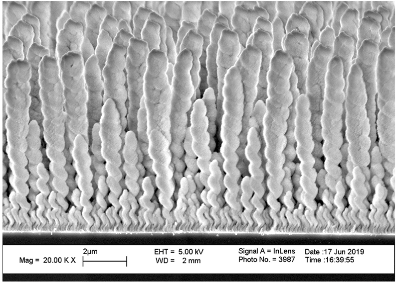
Sculptured Nano Forests (SNAFs)
Glancing angle deposition (GLAD), custom-built physical vapor deposition (PVD) operated at an incident angle > 80o with respect to the substrate normal, is employed to fabricate a close-packed array composed of separated nanopillars due to the self-shadowing effect and temperature-limited adatom diffusion. The deposited nanopillars consist of sculpturable shapes through controlling substrate movement, and are made of a wide range of materials (including metals, alloys, semiconductors and dielectrics). Such nanopillar arrays are so-called sculptured nano-forests (SNAFs).
Chiral nano-inorganics: to disclose the origins of biochemical homochirality
Many of life’s building blocks (e.g., amino acids and sugars) exhibit homochirality, with one stereoisomeric configuration preferentially existing over its mirror image, leading to chirality-dependent interactions and functions in biological systems. The existence of biochemical homochirality raises a fundamental yet unanswered question about the origin of molecular enantiopreference on Earth. One of the keys to answer this question is to understand external chiral forces to trigger symmetry breaking, which has been believed to induce the homochirality through chirality amplification. Symmetry breaking usually occurs in a stochastic manner, and chiral stimulations to trigger and control the symmetry breaking is ambiguous and under debate. Some external chiral forces have been proposed, including asymmetric mechanical forces, chiral electromagnetic fields and chiral organic-organic interactions. It is well known that organic life existed on the Earth made of inorganic minerals, so whether inorganic chiral materials could manipulate the symmetry breaking to result in the enantiopreferential homochirality? The investigation to answer this question is in its infancy.
We are devoting ourself to answering this crucial question using chiral nano-inorganics without attachment of chiral organic molecules, which are fabricated by GLAD. Chiral nano-inorganics, with the atomic and nano-scale chirality, are made of metals, alloys, semiconductors and magnetic oxides. Four kinds of external chiral triggers, associated with chiral nano-inorganics, are being under investigation, including chiral inorganic-organic enantiospecific interactions, chirality transmission from circularly polarized light, chirality transmission enhanced by superchiral near fields, and chiral-induced spin selectivity. Our works open a new door to disclose the origins of biochemical homochirality (or life), stemming from the chiral nano-inorganics on the prebiotic Earth.

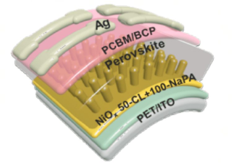
Optoelectronics
Semiconductor nanopillar arrays (NaPAs), functioning as charge transporting layers, can reduce light reflection loss, enhance the crystallinity of perovskites, prevent the decomposition of perovskites, suppress recombination dynamics, guide charge transport, and relax stress and strain in flexible optoelectronic devices. It leads to a significant improvement of photovoltaic performance, environmental stability, and mechanical robustness, for perovskite solar cells.
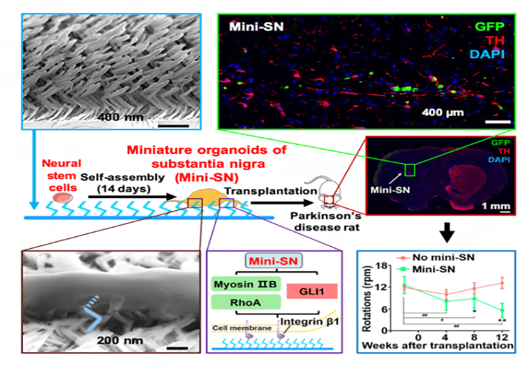
Inorganic Sculptured Extracelluar Nanomatrices (iSECnMs)
SNAFs made of biocompatible materials (such as silica) function as iSECnMs, to swiftly induce differentiation of neural stem cells (NSCs) to specific cell lineages. Diverse nanostructure-determined physical cues, such as matrix stiffness and topography, contribute to activating significant bio-signaling pathways of NSCs lying on the iSECnMs. Hence, engineering physical cues of iSECnMsleads to control the differentiated cell lineages. Furthermore, not applying traditional chemical growth factors result in minimizing the risk of carcinogenicity and tumorigenesis in vivoafter cell transplantation, paving the way for developing cell therapies to ultimately treat neurodegenerative diseases with no adverse effect.